Unlock Your IPhone’s Potential!
TodaysiPhone provides cutting-edge tutorials from tech experts that help you unlock your iPhone’s hidden capabilities and maximize its full potential. Discover tips to access secret features, optimize performance, and enhance productivity.

Latest Blogs


Don’t Miss the Latest Apple Innovations
Stay updated on Apple’s newest iPhone models, iOS updates, and product launches with TodaysiPhone’s timely, in-depth coverage. Our experts explain how each Apple innovation impacts your iPhone experience, so you understand the key improvements.

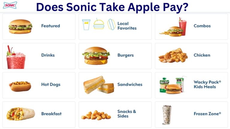
Master Seamless Payments with Apple Pay
The Apple Pay guides on TodaysiPhone provide everything you need to know to master this mobile wallet. Our step-by-step setup tutorial helps you securely add cards to Apple Pay. Learn where you can tap to pay with it at grocery stores, restaurants, transit stations and more. We explain how to manage your Apple Pay cards, use them for in-app purchases, ride transit and unlock all its features. Our Apple Pay blogs transform your iPhone into your payment method everywhere through comprehensive tutorials from TodaysiPhone.
Looking for something else? Use the search!
Browse our database containing hundreds of posts on Apple Pay, iPhone, and Apple devices.